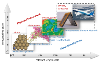
Phenomena, Scales and Simulation Methods
Specimen, devices and structures might look perfect and homogeneous. But usually there is a number of different physical phenomena on possibly a number of different length and time scales interacting among each other and giving rise to the so-called “micro structure”. For example, a metallic device might contain micro-cracks, may consist of a number of crystallographic grains, each of which contains kilometers of dislocation lines – that ultimately are related to displaced atoms.
 Understanding the relation between the microstructure
(e.g. grains) and the resulting property (e.g. yield stress or hardening) is the key for
designing new materials with superior properties.
Understanding the relation between the microstructure
(e.g. grains) and the resulting property (e.g. yield stress or hardening) is the key for
designing new materials with superior properties.
Simulations can guide experiments, help to identify new mechanisms and are able to test not yet existing materials in a “virtual lab“. This saves a lot of money in industry and leads the path towards new discoveries in research.
In CMS you will learn about both the physical phenomena and the respective simulation methods: On the atomistic nanometer scale this is the Molecular Dynamics methods that predicts how atoms move and interact. On the micrometer scale this can be dislocation dynamics or phase field simulations and on the macroscopic scale this is the discrete or finite element method.
Are such atomistic phenomena important for the resulting behavior of, e.g., micro chips or planes? Certainly, because in the end it’s the atoms that give rise to material properties! But this does not automatically mean that we plan to simulate a car or plane by MD simulations. Depending on what the phenomenon of interest is we may choose a different, much faster simulation methods and thereby intentionally neglect some phenomena.
You will learn to judge which information are dispensable and which are important. Only with this knowledge it becomes possible to judge the output of modern simulation methods.